Mains Powered White LED Lamp


Did it ever occur to you that an array of white LEDs can be used as a small lamp for the living room? If not, read on. LED lamps are available ready-made, look exactly the same as standard halogen lamps and can be fitted in a standard 230-V light fitting. We opened one, and as expected, a capacitor has been used to drop the voltage from 230 V to the voltage suitable for the LEDs. This method is cheaper and smaller compared to using a transformer. The lamp uses only 1 watt and therefore also gives off less light than, say, a 20 W halogen lamp. The light is also somewhat bluer. The circuit operates in the following manner: C1 behaves as a voltage dropping ‘resistor’ and ensures that the current is not too high (about 12 mA).
The bridge rectifier turns the AC voltage into a DC voltage. LEDs can only operate from a DC voltage. They will even fail when the negative voltage is greater then 5 V. The electrolytic capacitor has a double function: it ensures that there is sufficient voltage to light the LEDs when the mains voltage is less than the forward voltage of the LEDs and it takes care of the inrush current peak that occurs when the mains is switched on. This current pulse could otherwise damage the LEDs. Then there is the 560-ohm resistor, it ensures that the current through the LED is more constant and therefore the light output is more uniform. ..
Source link:http://www.extremecircuits.net/2010/07/mains-powered-white-led-lamp.html

LM339 based Grand Prix Starting Lights circuit


This circuit reproduces the starting light sequence currently used by FISA for Formula One racing. It could be used with slot car sets (such as HO scale AFX/Life Like/Tyco sets) or radio controlled cars. IC1, a 555 timer IC, is used as a clock pulse generator. Its output is fed via NAND gates IC2a and IC2c to IC3, a 4024 binary counter. IC2b inverts the O4 output of 4024 binary counter IC3. Initially, IC3 is reset and all its outputs are low, including O4, which causes IC2b to present a logical high to the pin 8 input of IC2c which then passes pulses from the 555 clock circuit to the clock input of the 4024. IC3 then begins counting.

After the count has reached binary 1111, the next pulse sends the O4 output of IC3 high, which disables IC2c and IC3 stops counting. The four used outputs of IC3 are connected to a resistor ‘ladder’ which acts as a simple digital to analog convert-er (DAC). As the count increases so does the voltage produced at the top of the ladder and this is connected to the inverting inputs of four comparators inside IC4 (an LM339) and to IC5, which is a 741 op amp also connected as a comparator.

The positive inputs of the comparators are connected to the taps of a voltage divider, with the tapping voltages set using VR1, a 100kO trimpot. As IC3 counts, the rising stepped voltage from the DAC ladder switches the comparators on in sequence, starting with IC4d and working up to IC5. As each comparator is turned on, its pair of LEDs is lit; first LEDs 1 & 2, then LEDs 3 & 4 and so on. When all five pairs of LEDs are lit, the next pulse from IC1 moves the binary count of IC3 to 10000, so the DAC voltage drops back to zero and all LEDs are extinguished. At the same time, counting also stops, because the high on O4 causes IC2c to block further gate pulses. The circuit then remains inactive until the counter is reset by pressing pushbutton switch S1. This allows a new sequence to begin.
Author: David Richards – Copyright: Silicon Chip Electronics
Source:http://www.extremecircuits.net/2010/06/grand-prix-starting-lights_12.html

IC-7805,7905 based Power Supply +5V to +25V, -5V to -25V 1A

IC-7805,7905 based Power Supply +5V to +25V, -5V to -25V 1A with

DC Voltage Regulator dual Power Supply +5V to +25V, -5V to -25V 1A with LM7805 LM7905

Here is Circuit Power Supply Regulator Adjustable Voltage Output +5 to +25V, -5V to -25V 1A ,Use IC 7805 for +Vout and IC 7905 for -Vout.
VR1 for Adjustable + Volt output,VR2 for adjustable -volt output.
Detail more see to circuit.

Variable DC Power Supply Voltage range 0.7 – 24V, Current limiting range 50mA – 2A

Voltage range: 0.7 – 24V

Current limiting range: 50mA – 2A

Device purpose:
A Variable DC Power Supply is one of the most useful tools on the electronics hobbyist’s workbench. This circuit is not an absolute novelty, but it’s simple, reliable, “rugged” and short-proof, featuring variable voltage up to 24V and variable current limiting up to 2A. It’s well suited to supply the circuits shown in this website. You can adapt it to your own requirements as explained in the notes below.
Parts:
P1____________500R Linear Potentiometer
P2_____________10K Log. Potentiometer
R1,R2___________2K2 1/2W Resistors
R3____________330R 1/4W Resistor
R4____________150R 1/4W Resistor
R5______________1R 5W Resistor
C1___________3300Î…F 35V Electrolytic Capacitor (see Notes)
C2______________1Î…F 63V Polyester Capacitor
D1,D2________1N5402 200V 3A Diodes
D3_____________5mm. Red LED
Q1____________BC182 50V 100mA NPN Transistor
Q2____________BD139 80V 1.5A NPN Transistor
Q3____________BC212 50V 100mA PNP Transistor
Q4 __________2N3055 60V 15A NPN Transistor
T1_____________220V Primary, 36V Center-tapped Secondary 50VA Mains transformer (see Notes)
PL1____________Male Mains plug
SW1____________SPST Mains switch
Device purpose:
A Variable DC Power Supply is one of the most useful tools on the electronics hobbyist’s workbench. This circuit is not an absolute novelty, but it’s simple, reliable, “rugged” and short-proof, featuring variable voltage up to 24V and variable current limiting up to 2A. It’s well suited to supply the circuits shown in this website. You can adapt it to your own requirements as explained in the notes below.

Notes:
P1 sets the maximum output current you want to be delivered by the power supply at a given output voltage.
P2 sets the output voltage and must be a logarithmic taper type, in order to obtain a more linear scale voltage indication.
You can choose the Transformer on the grounds of maximum voltage and current output needed.
Best choices are: 36, 40 or 48V center-tapped and 50, 75, 80 or 100VA.
Capacitor C1 can be 2200 to 6800uF, 35 to 50V.
Q4 must be mounted on a good heatsink in order to withstand sustained output short-circuit.
In some cases the rear panel of the metal box in which you will enclose the circuit can do the job.
The 2N3055 transistor (Q4) can be replaced with the slightly less powerful TIP3055 type.
Excellent quality-price ratio: enjoy!
source: RED Free Circuit Designs

Switching power supply Regulator 0-40V 4A by L296

Switching power supply Regulator 0-40V 4A by L296

Specificaly for the chip that is used in this circuit data are like this: Oscilator runs at freq 200kHz, output noise is below 1% (worst case), max current is 4A at 20V. Voltage can be regulated from 0,0 V (true zero), to 40 V. Voltage and current limit, can be adjusted. You should take special care when purchasing choke. Its ferrite material should be build for frequencies up to 300kHz. Input to the regulator can be DC or AC voltage – becouse the input is rectifier bridge.

Read more Source:http://www.peg.si/electro/switcher.html

TL783C based 48V PHANTOM POWER SUPPLY circuit with explanation

TL783C based 48V PHANTOM POWER SUPPLY circuit with explanation

This is a simple 48 V regulated linear power supply design that will provide up to 60 mA of current. This circuit is based on the Texas Instruments TL783C high voltage adjustable linear regulator IC, because this device will provide short circuit protection for an input to output differential voltage of up to 125 V. An LM317T can also be used in this circuit, but a short on the output will destroy the regulator IC. Protective diodes are included in this design to provide a discharge path around the regulator in case of an accidental reverse bias condition.

Part :
C1,C2,C3 – 220 uF 100 V
C5,C6 -10 uF 100 V
C6 -10 uF 100 VD1-D6 – 1N4002
R1 – 82 OHM 1/4 W
R2 – 1 K OHM TRIMMER
R3 – 2.7K OHM 1 W
T1 – 40 V at 0.15 A (6 VA)
U1 – TL783C


Source:http://members.aol.com/ecc81/ps48.html
thank you.

Victory Hammer (2008 ) Electrical Wiring Diagram

Victory Hammer (2008 ) Electrical Wiring Diagram
The Polaris Victory Hammer was first introduced in 2005. It is powered by a 100 cubic inches (1,600 cc) engine, 6-speed overdrive transmission, Brembo disk brakes, a Dunlop 250 mm tire on an 18-inch (460 mm) rim, and performance inspired inverted forks.

The following schematic shows the 2008 Victory Hammer Electrical . Herein you will find detail description of the electric parts/components of the motorcycle and engine harness splice location. Please note that all fuses, relays, and circuit breakers (except main 40A) are located in the fuse box under the right side cover.

Get more information about the 2008 Victory Hammer Electrical Wiring Diagram here (source: scribd.com)

2003 Suzuki DL1000 Radiator Schematic Diagram and Parts Components

Radiators are heat exchangers used to transfer thermal energy from one medium to another for the purpose of cooling and heating. The following schematic diagram shows detail of 2003 Suzuki DL1000 Radiator and its Parts Components which consist of 1. radiator assembly, 2. fan assembly, 3. cushion, 4. cushion, 5. spacer, 6. bolt (6×20), 7. shield, radiator heat, 8. bolt. 9. nut.

2003 suzuki DL1000 Radiator

Suzuki GSX R1000 (2005) Electrical Diagram

suzuki-gsx-r1000-electrical-diagramThe following article is about 2005 Suzuki GSX R1000 Electrical Diagram. Herein you will find detail yet brief information about electrical components, troubleshooting and inspection of charging system, starter system and side-stand/ignition interlock system, ignition system, combination meter, lamps (headlight, brake light, tail lights, and turn signals lamps), relays and battery (initial charging, servicing and recharging operation).

When performing the electrical service of GSX R1000, please pay attention on the following components:
Connector, when connecting a connector, be assure to push it until a click is felt, also inspect the connector for corrosion, contamination and breakage in its cover;
Coupler, with a lock type coupler, be sure to release the lock when disconnecting, and push in fully to engage the lock when connecting. When disconnecting the coupler, be sure to hold the coupler itself and do not pull the lead wires. Inspect each terminal on the coupler for being loose or bent. Inspect each terminal for corrosion and contamination.
Clamp, bend the clamp properly so that the wire harness is clamped securely. In clamping the wire harness, use care not to allow it to hang down. Do not use wire or any other substitute for the band type clamp.

Find the detail information of 2005 Suzuki GSX R1000 and here (44 pages of pdf file docs.)

Akrapovic Twin Exhaust System Schematic Diagram for 2009 SUZUKI GSX-R 1000

Akrapovic Racing and Evolution systems are designed for riders who demand maximum performance from their motorcycle. Both systems are significantly lighter if compared to stock exhaust system and feature exceptional production quality, hi-tech materials and of course increased engine performance combined with pure racing sound output.


The following file contains detail description and explanation on Akrapovic Twin Exhaust System for 2009 SUZUKI GSX-R 1000 and its schematic diagram. The system’s effect on the torque and power curve is huge and strongest in midrange rpm.

Get more info on Akrapovic Twin Exhaust System Schematic Diagram for 2009 SUZUKI GSX-R 1000 herefree download PDF file from Akrapovic.com

Suzuki GSX1300 Hayabusa Charging System Circuit (99 – 00)

Suzuki GSX1300 Hayabusa Charging System Circuit (99 – 00)
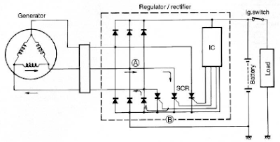
The circuit of Suzuki GSX1300 Hayabusa Charging System composed of generator, regulator/rectifier unit and battery. The AC current generated from the generator is rectified by the rectifier and is turned into DC current, then it charges the battery. While the engine rpm is low and the generated voltage of generator is lower then the adjusted voltage of regulator, the regulator does not function. However, the generated current charges the battery directly at this time.

When the engine rpm becomes higher, the generated voltage of the generator also becomes higher and the voltage between the battery terminals becomes high accordingly. When it reaches the adjusted voltage of the integrated circuit and it is turned “ON”, a signal will be sent to the SCR (thyristor) gate probe and the SCR will be turned “ON”. Then the SCR becomes conductive in the direction from point A to point B. At this time the current generated from the generator gets through the SCR without charging the battery and returns to generator again.


Suzuki GSX400F’82 Signal Generator Circuit Diagram

Suzuki GSX400F’82 Signal Generator Circuit Diagram

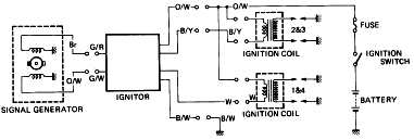
The 1982 Suzuki GSX400F signal generator is mounted on the right hand side of the engine in the area commonly used for contact breaker point. It is comprised of a magnet embedded rotor attached to a mechanical advance mechanism and two pick-up coils, with iron plates at their bases, affixed to a plate. Each pick-up coil consists of a coil of wire and a yoke or coil and is mounted, 180 degree apart on the plate. As the rotor magnet is turned past the coils, AC current is produced and used for switching within the transistor unit. The transistor unit controls power to the ignition coils and causes the spark plugs to fire at the proper time.

The following schematic shows the Suzuki GSX400F’82 Signal Generator Circuit Diagram:


Yamaha 175 Wiring Diagram and Electrical System Schematic

Yamaha 175 Wiring Diagram and Electrical System Schematic

The following picture shows the Yamaha 175 Wiring Diagram (CT2 and CT3 model) and Electrical System Schematic. Herein you get detail information regarding the interconnection and wiring between electrical parts and components of the motorcycle such as battery, ground, headlight, taillight, horn, rectifier, brake, flywheel magneto, etc.


Yamaha 175 Wiring Color Code

Daytime charging circuit
Night time charging circuit
Battery (+) circuit
Ground circuit
Front brake stop light
Rear brake stop light
Tail light
Head/meter light
Common circuit
Headlight main circuit
Headlight sub circuit
Horn circuit
Rectifier circuit
Flasher
Flasher light right
Flasher light left

Green
Green/Red
Red
Black
Green/Yellow
Yellow
Blue
Blue
Brown
Yellow
Green
Pink
White
Brown/White
Dark Green
Dark Brown

2005 Yamaha DT125X Wiring Diagram

2005 Yamaha DT125X Wiring Diagram
Generally the 2005 Yamaha DT125X electrical system consists of CDI unit, servomotor, battery, fuse, neutral switch, thermo unit, rectifier/regulator, ignition coil and main switch. You can find detail and complete 2005 Yamaha DT125X Wiring Diagram here on the last page of the service manual.

Yamaha DT250|350 Mikuni Carburetor Schematic and Diagram

The following Mikuni Carburetor Schematic and Diagram apply for Yamaha DT250 and DT350 series. The carburetor consists of following parts: pilot jet, float needle seat assembly, washer, o-ring, needle jet set bolt, needle jet washer, main jet, gasket, cover bolt, float, float lever arm, float pivot pin, float bowl gasket, float bowl, plate, float bowl screw, needle jet, throttle slide, clip, spring seat, throttle slide return spring, clip, carburetor cap, cable adjuster, etc.

Find detail diagram and schematics of Yamaha DT250|350 Mikuni Carburetor here – http://www.slimduck.com/dt250_dt360_carburetor.gif – source: slimduck.com.

Yamaha TDM850 (1996 )Wiring Diagram and Electrical System

yamaha tdm850 wiring diagram The Yamaha TDM850 is a Dual Sports or Adventure Sports motorcycle produced by Yamaha Motor Company of Japan, that first came out in 1991. The following wiring diagram and electrical system troubleshooting manual actually part of 1996 Yamaha TDM850 service manual. Herein you will find detail information regarding electrical system troubleshooting guideline and wiring diagram harness schematic of TDM850 which covers discussion on electrical components, switch inspection , ignition system circuit diagram and troubleshooting, electric starter system, starter motor, charging system, lighting system check, signal system wiring diagram, throttle position sensor self diagnosis.

The 1996 TDM850 electrical components consists of igniter unit, starting circuit cut-off relay, rectifier/regulator, main switch, thermo switch, thermo unit, flasher relay, starter relay, fuse box, battery, rear brake switch, sidestand switch, neutral switch, and ignition coil.

Find more info about 1996 Yamaha TDM850 Wiring Diagram and Electrical System here – http://www.carlsalter.com/aaman/Yamaha_TDM850_’96_Service_Manual.zip – free download PDF file

Yamaha Vino 125S Wiring Diagram


The following electrical system schematic shows the Yamaha Vino 125S Wiring Diagram. The electrical system consists of battery, CDI unit, carburetor heater, sidestand switch, horn, rectifier/regulator, ignition coil, rear brake light switch, starter relay, etc.


1 Main switch
2 C.D.I. magneto
3 Rectifier/Regulator
4 Battery
5 Main fuse
6 Battery (+) lead
7 Battery (-) lead
8 Wire lead
9 Starter relay
10 Starter motor
11 C.D.I. unit
12 Ignition coil
13 Auto choke unit
14 Front brake light switch
15 Rear brake light switch
16 Start switch
17 Engine stop switch
18 Starting circuit cut-off relay
19 Sidestand switch
20 Horn
21 Horn switch
22 Turn signal switch
23 Turn signal relay
24 Speedometer light
25 Tail/brake light
26 Dimmer switch
27 High beam indicator light
28 Turn signal indicator light
29 Fuel lever meter
30 Fuel sender
31 Headlight
32 Front turn signal light (left)
33 Front turn signal light (right)
34 Rear turn signal light (left)
35 Rear turn signal light (right)
36 Thermo switch
37 Carburetor heater

Wiring Color Code
B _ Black
G _ Green
L _ Blue
P _ Pink
R _ Red
W _ White
Y _ Yellow
Br _ Brown
Sb _ Sky blue
Or _ Orange
Ch _ Chocolate
Dg _ Dark green

.
B/W _ Black/White
B/R _ Black/Red
G/Y _ Green/Yellow
G/W _ Green/White
L/Y _ Blue/Yellow
L/W _ Blue/White
W/R _ White/Red
R/W _ Red/White
W/L _ White/Blue
Y/R _ Yellow/Red
Br/W _ Brown/White

Yamaha Virago Electric Starter Circuit and Wiring Diagram

virago electric starter wiring circuit diagram The Yamaha Virago Electric Starter system consists of starter motor, starter solenoid, starter circuit cutoff relay, starter cutout relay, sidestand relay, sidestand switch, neutral switch, starter button and related wiring. When the starter button is pressed, it engages the solenoid switch which closes the circuit. Electric current then flows from the battery to the starter motor. When the engine stop switch and the main switch are turned ON, the engine can only be started if the transmission is in NEUTRAL, or if the clutch lever is pulled in (transmission in gear) and the sidestand is up. If the above conditions are not met, the starting circuit is disabled and the starter will not operate.

Get the detail schematic of Yamaha Virago Electric Starter Circuit and here.

Photovoltaic Power System and Wiring Module Interconnection

Photovoltaic Power System and Wiring Module Interconnection


Photovoltaic (PV) is the field of technology and research related to the application of solar cells for energy by converting sunlight directly into electricity. The following Photovoltaic Power System manual is a suggested practices manual examines the requirements of the 2005 National Electrical Code (NEC) as they apply to photovoltaic (PV) power systems. In this manual you will get the design requirements for the balance-of-systems components in a PV system are addressed, including conductor selection and sizing, overcurrent protection device rating and location, and disconnect rating and location.

This manual is divided into sections which covers discussion on Photovoltaic Modules (including Modules Marking, Wiring, Module Interconnection, Tracking Modules, Terminals, Transition Wiring, Module Connection Access, Module Connectors, and Splices), Conductor Color Code, PV Array Ground-Fault Protection, PV Array Installation and Service, Grounding (including size of DC grounding electrode conductor, point of connection, charge controller, ungrounded system), Equipment Grounding, Inverter AC Outputs, Conductor Ampacity, Overcurrent Protection, Batteries, Generators, Charge Controller, Inverters, Stand Alone Distribution System, etc.

Copper conductors are recommended for almost all photovoltaic system wiring. Copper conductors have lower voltage drops and better resistance to corrosion than other types of comparably sized conductor materials. Aluminum or copper-clad aluminum wires can be used in certain applications, but the use of such cables is not recommended—particularly in dwellings. All wire sizes presented in this guide refer to copper conductors.

Find more information about Photovoltaic Power System and Wiring Module Interconnection in the following manual. (source: scribd.com)

Photovoltaic Transimpedance Amplifier Circuit Diagram

Photovoltaic Transimpedance Amplifier Circuit Diagram
The following schematic shows the Photovoltaic Transimpedance Amplifier Circuit Diagram. This design combines two Intersil X9258T digitally controlled potentiometers with an AD822 low noise dual op amp to create a flexible, digitally calibrated, wide dynamic range transimpedance amplifier topology that can be used with virtually any photovoltaic detector technology. The amplifier output is given by:

Vo = Is(1MΩ) ((1+P1)/(256-P1))

Where P1 is the 8-bit (0 to 255) digital value written to DCP1. For more detail information on Photovoltaic Transimpedance Amplifier Circuit Diagram, download the following file.

EPSON Stylus PHOTO RX600|610 RX620|630 Pinout Connector Diagram

The following table provides detail of EPSON Stylus PHOTO RX600|610 and RX620|630 pinout and .

EPSON Stylus PHOTO RX600|610 RX620|630 Pinout Connector Diagram

CN No.
CN3
CN4
CN5
CN6
CN7
CN8
CN10
CN11
CN12
CN13
CN14

Color
White
(FFC)
White
Red
White
(FFC)
White
Black
White
(FFC)
(FFC)

Pins
14
25
5
4
3
30
3
4
4
19
25

Connection Point
Power Unit
CCD Module
TPU Inlet Holder
Scanner Motor
HP sensor circuit board
Panel circuit board
Detector circuit board
CR Motor
PF Motor
Print Head
Print Head

Home Wiring Installation, Testing and Troubleshooting – a Complete Guide eBook

The following ebook you will find, provides a comprehensive manual for home wiring system from basic repairs to advanced projects.

home wiring installation ebook This ebook manual is divided into sections covering topics on Planning a Wiring Project, Circuit Maps for Common Wiring Layout, Basic (covers discussion on tools, materials and technique, electrical boxes for projects, installing electrical boxes, wires and cables for projects, installing NM cable, Conduit, Circuit Breaker Panels, Connecting Circuit Breakers, installing outdoor wiring, mounting the distribution centers, routing cables and wires, installing an , making final connections, testing the system and troubleshooting problems etc. Here is a quotation from the ebook:

An electrical circuits is a continuous loop. Household circuits carry power from the main service panel, throughout the house, and back to the main service panel. Several switches, receptacles, light fixtures, or appliances may be connected to a single circuit. Current enters a circuit loop on hot wires and returns along neutral wires. These wires are color coded for easy identification. Hot wires are black or red, and neutral wire are white or light gray.

Find more information about Home Wiring Installation, Testing and Troubleshooting - a Complete Guide eBook in the following Complete Guide to Home Wiring Diagram.

Electrical Wiring for Building – Standard and Code

Electrical Wiring Standard and Code Here is an article discuss on Electrical Wiring Standard and Code as used to provide power in buildings and structures, commonly referred to as building wiring.

The international standard wire sizes are given in the IEC 60228 standard of the International Electrotechnical Commission. This document and its precursors were created due to a need for a standard definition of cable conductor size. However, this standard is not written in such language that it can readily be adapted as a national wiring code.

Get more information regarding the Electrical Wiring Standard and Code here (reference: scribd.com)

ic-7805 based 5V breadboard mini PSU circuit with explanation

Micro PSU to power a breadboard with 5 volts. Connect to 9V battery, 12V or any other DC powersource from 8 to 18 volts. Follow the instructions on the site below to build your own mini 5V power supply.

5V breadboard mini PSU with 7805

Source:http://www.instructables.com/id/5V-breadboard-mini-PSU/?ALLSTEPS
Thank you.

7805 Datasheet - 5V DC Voltage Regulator Data Sheet / Specs

The 7805 provides circuit designers with an easy way to regulate DC voltages to 5v. Here are the the 7805 IC Datasheet and specification links that you need! Enjoy the Data Sheet!

Encapsulated in a single chip/package (IC), the 7805 is a positive voltage DC regulator that has only 3 terminals. They are: Input voltage, Ground, Output Voltage.

Although the 7805 were primarily designed for a fixed-voltage output (5V), it is indeed possible to use external components in order to obtain DC output voltages of: 5V, 6V, 8V, 9V, 10V, 12V, 15V, 18V, 20V, 24V. Note that the input voltage must, of course, be greater that the required output voltage, so that it can be regulated downwards.

General Features:
  • Output Current up to 1A
  • Output Voltages of 5, 6, 8, 9, 10, 12, 15, 18, 24V
  • Thermal Overload Protection
  • Short Circuit Protection
  • Output Transistor Safe Operating Area Protection
Full 7805 Datasheet Links:
  • 7805 Datasheet for Fairchild Semiconductors
  • 7805 Datasheet for KEC (Korea Electronics Company)
  • Source: electrokits.com/Datasheets/7805-Datasheet

78L05 / 7805 based +5V regulator circuit with explanation

This is a very simple article, just trying to help ….
What is the most vital piece we always need in electronics? The answer is …. a good power supply, right? :D .
The best regulators for using in electronic projects are the 78LXX (78L05, 78L09, 78L12, 78L15 … ). I searched google for the application notes and I found them easily (look in the bottom part of the page for the download link).
Their typical application was the IC + 2 small condensers (the input is at 0.33uF and the output is at 0.01uF), but after some tryouts and more googling I found this page which, too be honest with you, I consider it to be the best circuit over the web.
I tested the circuit and it worked like charmed.
Reading the application note we see that the input voltage must be between 7V and 20V and the output voltage is between 4.75V – 5.25V


Components:
  • IC1 = 78L05 / 7805
  • D1 = 1N4007
  • C1 = 100uF
  • C2 = 10uF
Bibliography :

Alkaline Battery Charger circuit with explanation


This circuit was specifically designed to recharge alkaline cells. The unusual connection of the transistor in each charging unit will cause it to oscillate, on and off, thus transferring the charge accumulated in the capacitor to the cell. The orange LED will blink for around 5 times a second for a 1.37V cell. For a totally discharged cell the blinking is faster but it will decrease until it will come to a stop when the cell is charged. You may leave the cell in the charger as it will trickle charge and keep it at around 1.6V. To set the correct voltage you have to connect a fresh, unused cell and adjust the trimmer until oscillations set in, then go back a little until no oscillation is present and the circuit is ready to operate. You should use only the specified transistors, LED colors, zener voltage and power rating because they will set the final voltage across the cell. A simple 9V charging circuit was also included: it will charge up to around 9.3V and then keep it on a trickle charge: the green LED will be off while charging and will be fully on when the battery is close to its final voltage.

A 2.5VA transformer will easily charge up to 4 cells at the same time although 2 only are shown in the schematic. In order to minimize interference from one circuit to the other they have nothing in common except the transformer and, in order to show a balanced load to the transformer, half of the charging units will use the positive sinewave and the other half the negative sinewave. Make sure to use high beta transistors such as BC337-25 or better BC337-40. Given the dispersion of the transistor parameters it might happen that oscillations do not take place. Use a slightly higher zener voltage: 7.5V instead of 6.8 or a green led in place of the orange ones.

All types of alkaline cells can be recharged: it will take 1 day for a discharged AA cell or 9V battery and up to several days for a large D type cell. The best practice is not to discharge completely the cell or battery but rather to give a short charge every so often although admittedly this is not easy to achieve. Do not attempt to recharge a totally discharged cell or a cell showing even the slightest sign of damage.

I tried successfully to recharge NiMH cells as well. Although the charging profile for these cells is quite different from alkaline cells, the circuit seems to work fine provided you do not leave them in the charger forever, because of the possibility of overcharging especially for the smaller batteries.

The mains transformer must be suited for the voltage available in each country: usually 230Vac or 115Vac.

Lie detector circuitwith explanation

Lie detector circuitwith explanation

Here’s a simple lie detector that can be built in a few minutes, but can be incredibly useful when you want to know if someone is really telling you the truth. It is not as sophisticated as the ones the professionals use, but it works. It works by measuring skin resistance, which goes down when you lie.

Here are the details of the specific parts you will need

Part Total Qty. Description Substitutions

R1 1 33K 1/4W Resistor
R2 1 5K Pot
R3 1 1.5K 1/4W Resistor
C1 1 1uF 16V Electrolytic Capacitor
Q1 1 2N3565 NPN Transistor
M1 1 0-1 mA Analog Meter
MISC 1 Case, Wire, Electrodes (See Nots)

Notes
1. The electrodes can be alligator clips (although they can be painful), electrode pads (like the type they use in the hospital), or just wires and tape.

2. To use the circuit, attach the electrodes to the back of the subjects hand, about 1 inch apart. Then, adjust the meter for a reading of 0. Ask the questions. You know the subject is lying when the meter changes.

http://www.aaroncake.net/circuits/lie.htm

LA3161 based Preamplifier circuit with explanation

LA3161 based Preamplifier circuit with explanation


Preamplifiers are used to amplify low level signals such as those from mikes, tape heads before they are fed into power amplifiers. Power amplifiers are generally less sensitive. Frequency response also can be suitably trimmed and modified at preamp stage. LA 3161 is one of those widely used in tape decks and amplifiers as a stereo preamplifier.LA3161 based Preamplifier circuit with explanationLA3161 based Preamplifier circuit with explanation


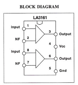
Block Diagram is shown in Figure. LA 3161 has two low noise preamplifiers with good ripple rejection on chip catering to stereo applications. External part count is low and Single In line (SIL))(Figure 43) package makes mounting easy. Wltile the operating voltage is 9V, the IC can tolerate voltages up to 18V. Typical input resistance is WOK and output resistance is 10K with an open loop gain of78dB. Block diagram of the IC is given below. Input is given at Pin 1 and 8, output is taken at Pin 3 and 6, and negative Feedback is given at Pin 2 and 7. Power is at Pin 5 and Pin 4 is the ground terminal. There is an internal voltage regulator.

Ready made PCBs, even populated PCBs are available using this very useful IC. You can still build one, with a Veroboard provided proper care is taken about the ground returns. It simply means that one should not connect ground terminals of output and input at the same place. This will create serious oscillations and normal hobbyist will be left in the woods. Please read general instructions for working with amplifiers in the end.

LA4555 based Audio Amplifier circuit with explanation

LA4555 Audio Amplifier mono circuit 300x276

LA4555 Audio Amplifier mono circuit1 300x276

Stereo circuit and mono circuit are given in schematic .LA 4555 is basically a stereo amplifier with 2.3 watts into 4 ohms speakers at a total distortion of 10%. With a bridge circuit, it can be configured as mono amplifier delivering 4.6 watts. It has an input impedance of 30K and gain of 51 dB. It has an excellent voltage range of 3 to 13 volts. Both mono and stereo circuits are shown here.

Pin out is given in Figure

LA4555 top view 300x165

Input is given at Pin 8 in the mono circuit and output is taken at Pin 11 through a capacitor (C7) of 470 uF to a speaker of 4 ohms. In the case of stereo circuit, input is given at 5 and 8 pins and output is taken out at 2 and 11 pins respectively for left and right channels through the blocking capacitors C4 and C7.

A detailed description of the pin out will help now and in the future.

In the stereo circuit,

C5, C2 are feedback capacitors, zohich dictate the lower cut off frequency.

CI, C6 are bootstrap capacitors. If the capacitor value is reduced from the recommended 47uF, output

at flow frequencies falls.

Cll, CIO are oscillation blocking capacitors. Polyester film capacitors are preferable.

C7, C4 are output coupling capacitors. Lower cutoff frequency depends on their value and quality.

C3 is the ripple filter or decoupling capacitor.

C8, C9 are the power source capacitors.

R2, R2 are oscillation blocking resistors.

ICs dissipate heat as they dissipate more and more power at more and more voltages. The heat must be removed continuously such that IC operates at rated temperature. Failure to do so will result in thermal runaway. If the IC is well protected, output power will fall to a safe area. If not it will eventually fail and pack up. Copper foil area is made as large as possible in the vicinity ofIC to dissipate more heat.

Then heat sink, thermally conductive material such as copper or aluminum is mounted on IC to remove the heat as it develops. It must be of enough size. In case ofLA4555, the IC has fins which are soldered to the PCB and a small heat sink also can be soldered along with it. Solder copper heat sink as shown in the figure below. Aluminum cannot be easily soldered. Method of mounting heat sink is shown in Figure.

heat sink mounting 300x149

readmore: www.engineeringslash.com/audio-circuits/la4555-audio-amplifier.html

Webster TP45 17dBW PA amplifier, 2 6L6GC schematic

Webster TP45 17dBW PA amplifier, 2 6L6GC schematic
www.angelfire.com/vt/audio

Webster 95B25 14dBW PA amplifier, 2 6L6 schematic

Webster 95B25 14dBW PA amplifier, 2 6L6 schematic
source: angelfire.com/vt/audio

Hammond Organ Type E 16dBW main amplifier, 2 7591A schematic

Hammond Organ Type E 16dBW main amplifier, 2 7591A schematic
source: angelfire.com/vt/audio

Grommes-Precision-Frazier G-101A, F-106C 20 dBW power amplifier, 4 6GT5 schematic

Grommes-Precision-Frazier G-101A, F-106C 20 dBW power amplifier, 4 6GT5 schematicsource: angelfire.com/vt/audio/

Digital Countdown Timer


The presented digital timer is built in addition to the before mentioned ultraviolet light box.
Indication is on 4 digits seven segment LED display.
The timer counting backwards from 99 minutes and 59 seconds to 00:00.
It is built with microcontroller PIC 16F84A and integrated circuit CD4511.
Supply for the ultraviolet LED diodes are terminated with the help of the electromagnetic relay 6Volti.
Set the countdown time is done with 2 command keys, and the timer starts with the tally.


Author:Petar Avramovski

Source: Magazine Emiter

L4970A Easy 5V 10A Switching Regulator circuit


Friends that seek 5V 10A power supply circuit small-sized and build easy. I begs for to advise this circuit. It is 10A switching regulator by use IC L4970A. Then build easy as an example integrated readymade circuit. Important point be power supply input must have 10A current sizes then can give power get enough.

The detail is other of the circuit almost must not fine to decorate anything. If friends take an interest try seek buy the integrated circuit and other equipment. come to try build immediately yes.
Image Circuit from www.st.com site.

IC TDA7012T Mini FM Received Based on Single FM circuit with explanation

 IC TDA7012T Mini FM Received Based on Single FM circuit with explanation
Mini FM Received Circuit

TDA7021T chip radio receiver ambit is for carriageable radios, stereo as able-bodied as mono, area a minimum of ambit is important in agreement of baby ambit and low cost. It is absolutely accordant for applications application the low-voltage micro affability arrangement (MTS). The IC has a abundance bound bend (FLL) arrangement with an average abundance of 76 kHz. The selectivity is acquired by alive RC filters.

The alone action to be acquainted is the beating abundance of the oscillator. Interstation babble as able-bodied as babble from accepting anemic signals is bargain by a alternation aphasiac system.

Part List:

R1 = 8kΩ2
R2 = 10kΩ
R3 = 390Ω
C1,C3 = 10nF
C2,C6,C9,C16 = 100nF
C4 = 33pF
C5 = 25pF trimmer (Murata type TZB4Z250AB10R00)
C7,C10 = 1nF5
C8 = 820pF C11 = 1nF
C12 = 68pF
C13 = 220pF
C14 = 47μF 10V (Nichicon UWX1A470MCL1GB 5.5mmL chip type)
C15 = 3nF3
L1 = 36nH (4 turns 0.5mm silver-plated wire, inside diameter 4mm; length 7mm)
L2 = 1μH, SMD case 0805 (fres > 300 MHz)
IC1 = TDA7021T (SMD in SO16 case)

12 Volt 20 Ampere Regulator circuit with explanation

12 Volt 20 Ampere Regulator circuit with explanation

A heavy duty 13.8V power supply is a fine thing to have in the shack, but unless you acquire one secondhand, is an expensive little beastie to buy. This means building one should be considered, not only for the cost savings, but also because you can brag about it on air to your mates. Of course, careful consideration must be given to the properties of the completed supply, and after talking to a few of my friends who have built their own and fallen into all the traps, here are the printable ones : RF proof, easy to make, commonly available parts used, but above all CHEAP.

Well, last things first. Breaking down the construction costs of a heavy duty regulated supply, they are in order:

  • The transformer (around $A80)
  • The main filter electrolytics – around $A80
  • The case – a metal case is well beyond the workshop capabilities of many amateurs and is quite expensive to buy (if you can).
  • The meter – around $A20-$27 (either digital or analogue)
  • The electronics – transistors, resistors, diodes, etc.
  • All the bits – fuseholders, terminals, switches, solder tags, nuts and bolts, power cords, etc.
  • 7812 and 7912 Dual Regulator circuit with explanation


    Voltage Regulators low ability burning IC 78W alternation acclimated in our chart is now so bargain they are an economical another to simple regulators NPN-stabilizers. In addition, they action the allowances of bigger regulation, accepted absorbed / abbreviate ambit aegis to 1000 mA blow and calefaction bottomward if the electricity disperses too. Indeed, is not the alone way for these drives can be damaged polarity is incorrect or boundless ascribe voltage. RegulatorsAlternation 78W to affectionate of break 8V ascribe voltage of about 35V, while the blazon 24v bear 40V. Of course, of course, that regulators will not assignment with such an important ascribe cogwheel achievement as it would advance to boundless ability is dispersed. All controllers will bear the 78Walternation 1000mA accepted best accepted ascribe cogwheel voltage achievement of beneath than 7V. Otherwise, too broadcast power, thereby bringing the blaze extinguished.

    Two transformers were acclimated to footfall voltage 230-250V AC ascribe power. It articles ability transformers 6-0-6V accessory terminals. This achievement is fed into the rectifier and clarify capacitor. Filtered IC6 that served 3-pin voltage regulator that provides a adapted achievement + 5V. It is acclimated to accredit the DPM system. It additionally comes as the arrangement voltage antecedent temperature accuracy.

    Other articles transformers with a accommodation of 12-0-12V at its accessory terminals. The centermost was accustomed as a bubbler in the antecedent case. The added two accessory terminals are fed archrectifier complete application diodes. Achievement recovered is filtered application a capacitor C5 and C6 for aliment and IC7 IC. In-8 IC7, which are 3-pin regulators accommodate achievement voltage of ± 8V. These two voltages are arresting generator. TO-8V ability antecedent is activated to the temperature of the network, and the advertence voltage. It is additionally all-important to +12 V and-12V food for the accomplishing of operational amplifiers. This can be calmly done application a 12V zener diodes. The achievement of archrectifier is absorbed to the +12 V and-12V, respectively, application two zener diodes. In the zener achievement is fed to the terminals of the operational amplifier supply. For supply

    for operational amplifiers charge not be actual able in acclimation + 12V, the use of Zener diodes be costly.

    For the testing of cyberbanking apparatus voltage aloft 50 V is required. This can be accomplished through quadruple the alternation tension. It consists of four diodes and four electrolytic capacitors. Unreasonable Administration Accessory 12-0-12V is affiliated to quadruple string. Quadrupled achievement of the ambit is 68V to ground.

    2N3055, Power Circuit Inverter : 300W Inverter power 12V to 220V circuit with explanation

    Inverter 12V to 220V 300W NE555,2N3055
    This in power inverter circuit the size about 300W .It performs to transform from battery 12V be house electric 220V 50Hz by have signal picture is Square wave. And it has the distinction that uses the equipment seek easy, such as integrated circuit NE555 and 2N3055 transistors. request to have fun circuit this idea.
    http://schematiclabs.info/wp-content/uploads/2010/02/power-inverter-300w-300x139.jpg

    Typical Throttle Position Sensor Circuit Diagram

    Here is a typical schematic diagram of the car Throttle Position Sensor Circuit. The Throttle Position Sensor (TPS) is designed to indicates the position of the throttle valve. Usually the Throttle Position Sensor is mounted on the throttle body and converts the throttle valve angle into an electrical signals. Inside the TPS is a resistor and a wiper arm. The arm is always contacting the resistor.
     Throttle Position Sensor Circuit Diagram
    How the Throttle Position Sensor works?
    A wiper arm inside the sensor is mechanically connected to a moving part, such as valve or vane. As the part moves, the wiper arm also moves. The wiper arm is also in contact with a resistor. As the wiper arm moves on the resistor, the signal voltage output changes which indicates position.

    Fuel Tank Pressure Sensor Circuit with explanation

    The control module monitors the fuel tank pressure (FTP) sensor signal in order to detect vacuum decay and excess vacuum during the enhanced evaporative emission (EVAP) diagnostic. The responds to changes in the fuel tank pressure or vacuum. This information is used in order to detect vacuum decay or an excessive vacuum during EVAP diagnostic routing. The fuel tank pressure sensor signal voltage to the VCM varies from a minimum of about 0.1 volts with pressure in the fuel tank to above 4.0 volts with a high vacuum in the fuel tank.

    The following schematic shows the Typical Fuel Tank Pressure Diagram.
     Fuel Tank Pressure Sensor Circuit with explanation

    single supply NE5532 preamplifier circuit

    By the people's suggestion I bought myself a breadboard and decided to implement simple (I would even say trivial) single-supply NE5532 chip preamp. Let's see what was done.


    Single-supply NE5532 chip preamp made on the breadboard

    Single-supply preamp schematic
    I dropped PSU filters and Zenner diode voltage limiter, since used lab PSU with 15 V voltage.
    'Amplifying' resistors are selected to be the same (and thus preamp actually becomes a real one with amplifying ratio equal to 2) and to be equal to the input chain resistance (single supply shift made as resistor-based voltage divider and input resistor) to minimize bias current. That's why there are so many resistors on the actual scheme to match resistance.
    Now the results.


    Square wave signal
    Square wave signal has noticeble peaks at the edges, let's see them in details


    Square wave signal peak details
    Given the huge amplitude of the input signal (more than a volt) this may be not a limiting factor actually.
    What is a real problem, is the input signal range as a whole. Since I used 15V as a supply voltage, its inner ground will be roughly at 7.5 V (there is an appropriate voltage divider attached to the non-inverting input signal), so having total output amplitude of 4 V may be not appropriate for the chip operational amplifier.


    Big sine signal cut
    Experiments showed that this chip preamp operates correctly when resulted output signal does not exceed 1/10 of the supply voltage (i.e. about 1.2 V max). Triangle and sine signals after some level (when input signal amplitude is about 3-4 V) start producing reversed output signal in the cut area above, i.e. in the middle of the cut line small sine or triangle signal starts growing.
    Now question, why do we need chip preamp for the chip amplifier? I believe that the main reason for preamp is to allow to connect power amplifier which may have not very high input resistance, so small preamp with good characteristics (like huge input resistance and very small output one) will not distort small enough input signal. But I think that most of the modern chip sound amplifiers like LM3886 already have big enough input resistance (as all others they have differential amplifier as the first cascade), maybe not that high if would be built with field-effect transistors, but I wonder if that is ever noticeble.
    http://www.ioremap.net/node/141