Showing posts with label Schematics. Show all posts

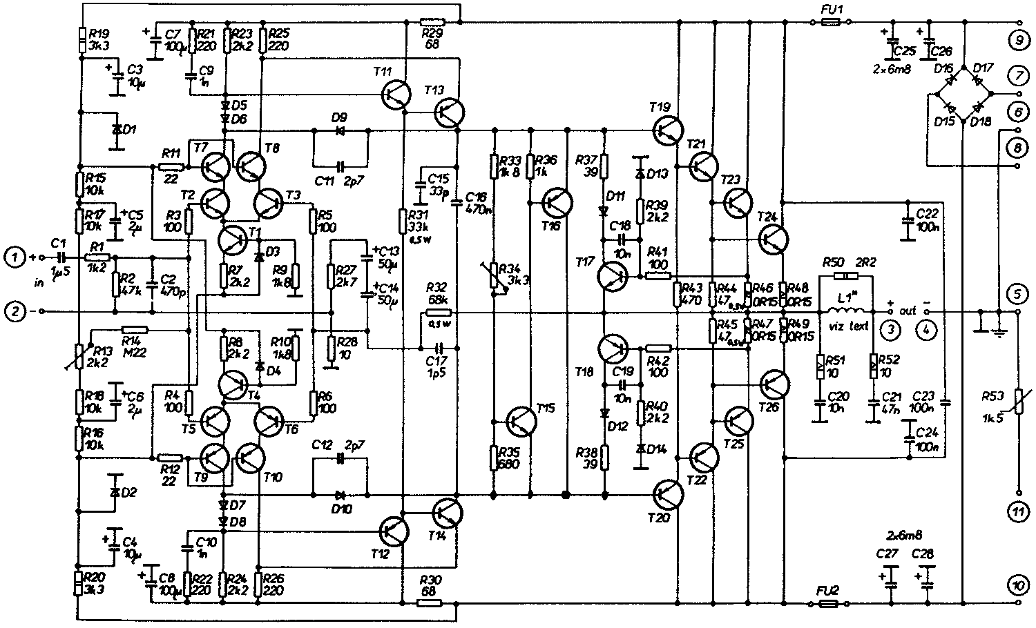
The DPA 220 schematic
The DPA 220 schematic


The DPA 220 low detail schematic (click on the image to see the high detailed version (47 Kb)

Do not try to print this picture in Netscape because it's too big.


T1 to T6 create the input differential stage. The D7 and D8 zener diodes stabilize at 5V. These are just the simplest low-power zeners, only they have to be coupled in tolerance of 200 milivolts, which should not be a problem. T1 to T6 are common all-purpose low-power transistors with high Hfe. These six and maybe the next four have to be coupled in tolerance of 25%.

The T7 and T8 are fast, switching application types.

T9 and T10 have to be fast and must hold a high voltage, thus the best are the "video" types - BF469/470. T15 and T16 are the same types.

The C9, C10 and C15 should stand voltages higher than usual 50 V - I don't know why.

D3 to D6 can be any silicon type, not Scottky, the ones listed below are just all-purpose low-current ones for 150 V. These diodes should be rather fast - "switching types".

The T11 and T12 stabilize the BIAS current for the power stage. T11 also serves as a temperature sensor, and is mounted to the cooler of power transistors.

T13 and T14 secure the output current - in cooperation with R38 and R39.

The output transistors used here are Tesla types - Tesla is a former local devices manufacturer - the pair in each branch can be replaced with a single power darlington, like BD649/BD650. They should have Pc > 150W, Ic > 15A, Uceo > 100V.

In this case obviously the R38+R40 / R39+R41 must be connected parallel. These resistors should be able to absorb high power - at least 2 W, but I'd use 5W ones.

The output filter improves stability of the amp when working with complex impedance of speakers - it is quite important. The resistors are high-power ones again, the coil is 13 turns of a 1.2 mm wire on a 8 mm thorn (diameter). R43 is placed coaxially in the coil.

The schematic also includes power supply capacitors and rectifier - the capacitors' size is not crucial, generally the bigger the better. The rectifier originally consists of four silicon 10A diodes, but you can use whatever you have - rectifier bridge etc. The trafo should be a 2 * 30 V / 7 A type so that you have +/- 40 V on the power supply capacitors.

In the scheme there's also a thermistor that is supposed to be connected to some additional circuits that secure temperature and other things.
The complementary input stage of DPA amps is an unmistakable heir of earlier designs published by Mr. Borbely in several issues of Volume 1984 of the Audio Amateur.
source: http://english.cxem.net/amplifier/amplifier1.php

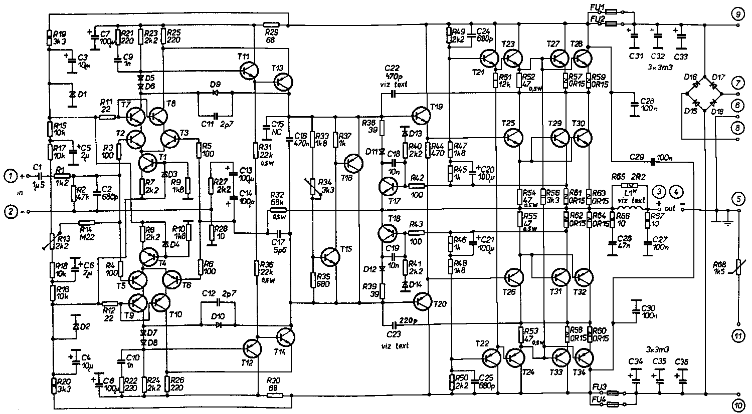
The DPA 440 schematic


The DPA 440 low detail schematic (click on the image to see the high detailed version (47 Kb)

Do not try to print this picture in Netscape because it's too big.


This amp is just a more powerful brother of the above. The output transistors are not darlingtons anymore.

The bias current is 55 mA. The output coil is 16 turns of 1.5mm wire on an 8mm diameter.

The best visible difference is seen in the input stage - the differential amp has 5 transistors in each branch instead of three. The two additional transistors, T7+T8 / T9+T10, take over the voltage, while the rest is responsible for the amplification. The T1 to T6 don't have to carry the high voltage and can be low-noise types, while T7 to T10 carry the voltage.

The author says there's another important advantage - this solution subdues Miller's feedback CB capacities of the differential amplifiers which improves slew rate and thus distortion on high frequencies.

Also the transistors of the differential amplifier work at a constant voltage which improves linearity and th us contributes to lower distortion.

The trafo should be about 2*40 Volts and 12 to 15 Amps.
source Read more at
http://english.cxem.net/amplifier/amplifier2.php

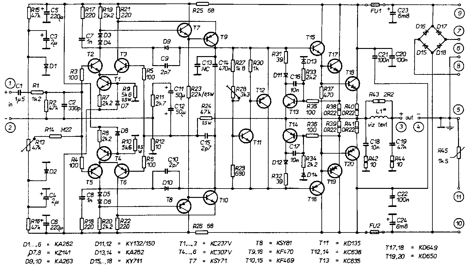
The DPA 880 schematic


The DPA 880 low detail schematic (click on the image to see the high detailed version (48 Kb)

Do not try to print this picture in Netscape because it's too big.


Nothing much to discuss here :


Again, this one is similar to the above ones, only it uses serial connection in the power stage to allow a higher voltage.
The bias current is 110 mA.
The output coil is 14 turns of 1.8mm wire on an 11mm diameter.
The trafo should be about 2*57 Volts and 20 to 25 amps !!!
source read more at
http://english.cxem.net/amplifier/amplifier3.php

Net-Enabled Alarm Clock Unlike old-school mechanical alarm clocks that you have to set manually, DJ’s Internet-connected alarm clock provides three p


Unlike old-school mechanical alarm clocks that you have to set manually, DJ’s Internet-connected alarm clock provides three primary features: automatic time setting on power-up, streaming MP3 music, and remote management. The PIC24FJ64-based clock is connected to an ENC28J60 Ethernet chip, an MP3 decoder chip, an organic LED graphical display, and a 24LC512 EEPROM for storage.


Most alarm clocks use a radio, beeper, or CD player to wake you up. My clock accesses my MP3 collection on the server in my home office via an Ethernet port. The network connection enables me to remotely manage the clock as well. I can easily set alarms and choose music from my office without waking up my wife. The clock also has a built-in GUI so I can manage it locally. Its OLED display and photocell enable it to adapt to different lighting conditions (from bright sun to pitch black).


Now you too can build a customized alarm clock. In this article, I’ll describe the design process from start to finish.


Source: Copyright DJ Delorie

A Tiny pH-Meter This electronic circuit is a tiny pH-meter. It is very tiny: 11cm2 including the PSU circuit! The schematic is shown below. It is bas

A Tiny pH-Meter

This electronic circuit is a tiny pH-meter. It is very tiny: 11cm2 including the PSU circuit! The schematic is shown below. It is basically a simple gain/offset circuit with a high impedance input (several giga-Ohm) and frankly the explanation could stop here: anyone with an background in electronics can understand this. But I started to write a webpage about this, so let's try to do it right and describe the schematic.


Juste because it's damn small does not mean that you have to settle down for second best when it comes to performance. The repeatability is around 0.01 pH and the accuracy, while depending on how well you will calibrate it, is around 0.02 pH. The main characteristics are:

  • very small footprint (11cm2)

  • very lightweight

  • pluggable module for easy replacement

  • requires only an external transformer and a display unit to work

  • slope/offset settings

  • repeatability 0.01 pH

  • accuracy 0.02 pH

  • low power

  • low-cost single-sided PCB

  • total unit price (including case and display unit): less than 100 euros.


The circuit input is pin 15 of K1. The probe signal enters IC1 via an RC circuit designed to allow only relatively slow signal variations (and avoid getting parasite HF signals). IC1 is a CMOS op-amp and thus has a very high impedance. The gain of IC1 is adjusted with the potentiometer R14. C2 is there for the amplifier stability. The R5/R11 circuit is the adjustment of the amplifier offset which is necessary for a high-precision application like this (see calibration below).

Once the signal has been amplified it enters an offset circuit built around IC2. IC2 is a more classic TL081 op-amp commonly found in audio devices, among others. The offset is defined by two potentiometers R12 and R13. The first one is on the PCB and the second one on the front panel. This improvement on the original design (single pot) allows the range swept by R13 to be symmetric, albeit smaller than without R12. It can be skipped if you wish (those small SMD trimmers can be damn expensive...). The circuit is designed to provide an average offset of 2V.

After the offset circuit the signal passes through a voltage divider before reaching the display unit. The divider roughly changes the signal range to something that is acceptable for the display. The real setting will be done on the display itself which contains a multiturn trimmer to precisely adjust its input gain.

The voltages for the signal evolve in the circuit as follows:

  • Before IC1: -0.414/+0.414V (this might depend on the electrode used and its age, hence the gain/offset control)

  • After IC1: -2/+2V

  • After IC2: 0-4V

  • After the voltage divider: 0-140mV (roughly)

  • After the on-display trimmer: 0-140mV

  • On the display: 0.00 - 14.00 pH (the display measures mV but the decimal point is placed accordingly to show a 0-14pH range)

As you can see the electrode voltage is symmetric and must undergo a linear transformation to fit the 0-14 pH range. This is all very classic stuff... Note that even if the supply rails are at +/-5V the circuit can cope with a 0-4V signal because the output swing is almost equal to the rails (no 0.7V drop, more around 0.3V IIRC).

A little remark concerning the integrated power supply circuit: it is a very small circuit that supplies a maximum of 50mA. Be careful of you want to add a power LED or something like that as it might be too much for the circuit. Check the total power used by the circuit before adding extras.

PCB

The PCB is very small and you are advised to build it with through-hole mounting components if you're not familiar with SMDs. That means start the PCB design from scratch. I personally think that it looks much cooler with a small footprint... No other special remarks concerning the PCB, except that the PCBs that were manufactured were slightly different (see the photos below). This is actually also true for the schematic. No functional difference, but I changed from Protel to Eagle for designing the circuit so I had to reenter the schematic and PCB manually. Hence some differences in layout but this is not a big deal.


Component list

This is the list of components used in this circuit. I only mention the display and probe at this time as the other components are generic. Maybe more info will follow in the future.


A little link to the display unit used in this project. I chose this one because it has a nice 'pH' unit that can be activated on the display.


Another link to the probe used with this circuit (IIRC). Most probes should work but I only tested the circuit with this one.

Construction


Random remarks: start with the smallest components, go slow, don't forget to set all the solder bridges correctly on the display unit (what you want is a 0-200mV range, an appropriately set dot and 'pH' shown as the unit). Check your cables,... before powering up.


The cabling diagram of K1 is:

* 1: AC 1

* 2: GND

* 3: +5v OUT (to display)

* 4: SIGNAL OUT (to display)

* 5: R13 / 2

* 6: R14 / 1

* 7: -5V OUT

* 8: R14 / 3

* 9: AC 2

* 10: GND (from transformer)

* 11: GND (to display)

* 12: GND (to BNC input)

* 13: R13 / 1

* 14: R14 / 2

* 15: INPUT


Source: ©Damien Douxchamps